A better register
In entry 9, we created QuadDFlipFlop, a first version of a register. Starting from this design, let's replace the ungated D flip-flops with gated ones, and add four tri-state buffers to the output pins. We then have a register we can connect to a data bus.
Here is the schematics of what I will build.
This component will be called a FourBitRegister, see ACEL.
- D0-D3 are data input pins, connected to the data line D of the D flip-flops.
- Load is an input pin, controlling all the gates of the D flip-flops.
- Clear is an input pin, setting all the D flip-flops to Q = 0.
- Clock is an input pin, a common clock signal for all the D flip-flops.
- Write is an input pin, a common "enable" for all the tri-state buffers.
- Q0-Q3 are output pins, the data stored in the D flip-flops. These are not tri-state.
- W0-W3 are tri-state output pins. When Write = 0 they are in state Z ("disconnected"). When Write = 1, W = Q.
74LS173
The design of FourBitRegister is very similar to 74LS173/74HC173:
- 1D-4D are the "D0-D3"
- 1Q-4Q are teh "W0-W3)
- M and N together is the "Enable"
- G1 and G2 together is the "Load"
Moving data from one register to another using the data bus
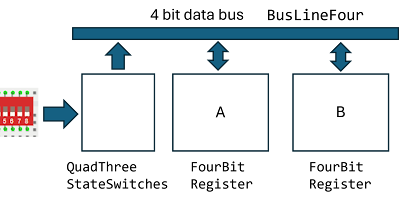
To test this out, we connect two registers (A and B) to a data bus. The goal is to move data from register A to register B. We also need DIP-switches to get data onto the bus (through tri-state buffers). This is the schematics.
Code:
Try this out yourself on Wokwi, project "Two registers and a bus".


No comments:
Post a Comment