Friday, April 4, 2025

Entry 23: Combining memory system with ALU

Memory system

In entry 21 we built a memory system consisting of 16x4 RAM, an MDR (Memory Data Register), a MAR (Memory address Register) and two MUX's. This allows RAM to be hooked up to either buses or DIP's:

I combined these 5 components into one chip called "SixteenByFourMemorySystem": It has the following pins:

  • MARD (4): D pins of MAR, connection from the address bus.
  • DIPA (4): Connect to address DIP's
  • MDRD (4): D pins of MDR, connect from the data bus.
  • DIPB (4): Connect to data DIP's
  • WA (4): To the address bus (tri-state), W pins of MAR and RAM
  • WD (4): To the data bus (tri-state), W pins of MDR and RAM
  • Two pins to set source of address and data in RAM:
    • SA: Select pin of address MUX (left)
    • SD: Select pin of data MUX (right)
  • 6 control pins + clock:
    • MARL: Load pin of MAR
    • MARW: Write pin of MAR
    • MDRL: Load pin of MDR
    • MDRW: Write pin of MDR
    • RAML: Load pin of RAM
    • RAMW: Write pin of RAM

Testing the ALU

In the previous entry, we designed the simplest version of an ALU, one that can add two 4-bit numbers A and B:

I want to try this out in combination with the memory system. This is the test I want to perform:

  1. Use the DIP switches to program RAM. Program address 0: 5 and address 1: 3.
  2. Move the content of address 0 (the number 5) to a register named A.
  3. Move the content of address 1 (the number 3) to a register named B.
  4. Hook up to ALU, which will calculate the sum (the number 8).
  5. Store the sum in RAM at address 2.

This is what we need to hook up:

These are the chips used for this test:
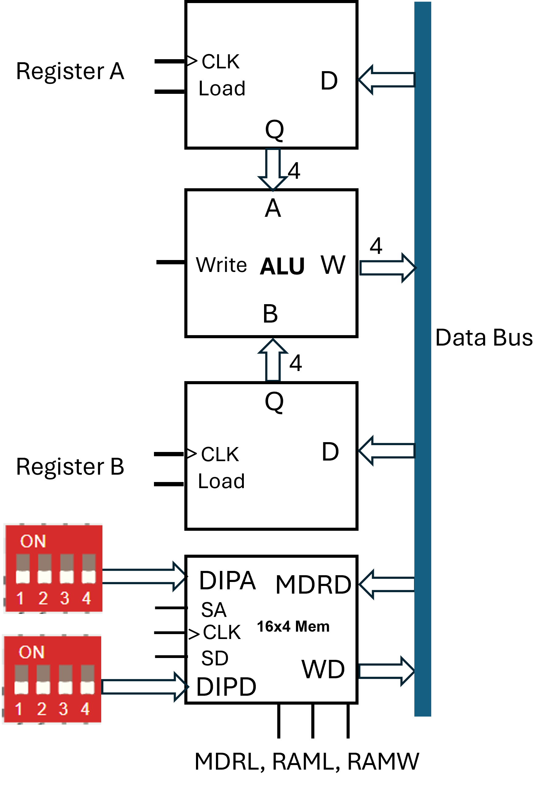
  • "SixteenByFourMemorySystem", see above
  • Two "FourBitRegister", see entry 15
  • "FourBitAdderTriState", see entry 22

Controls and DIPs:

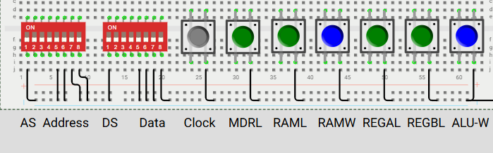
Try this out yourself at Wokwi, project "Testing the ALU", where you can see all the connections. We can confirm that the setup is working as expected by performing the following steps:

  Testing the ALU
  1. Use the DIP switches to program RAM. Put say 5 at address 0 and 3 at address 1.
  2. Move the content of address 0 to Register A (the number 5)
  3. Move the content of address 1 to Register B (the number 3)
  4. The ALU will calculate the sum (the number 8)
  5. Store the sum in RAM at address 2.

  Step by step:
    Set DIP 1 to ON on the address DIP's (left)
    Set DIP 1 to ON on the data DIP's (right)
    This takes us into "programming mode" where the DIPs determine address and data  
    Program: 5 at address 0, 3 at address 1:
      Set address DIPs to 0000
      Set data DIPS to 0101 (decimal 5)
      Click RAM-L
      Similarly for address 1
    Click Print. Observe RAM and that correct data has been programmed.
    Move the content of RAM at address 0 to register A
      Set address DIPs to 0000
      Click and hold RAMW, REGAL (press 4 and 5 on keyboard)
      Click Clock to latch
    Click Print. Observe Register A and that Q = 5
    Move the content of RAM at address 1 to register B
      Set address DIPs to 0001
      Click and hold RAMW, REGBL (press 4 and 6 on keyboard)
      Click Clock to latch
    Click Print. Observe Register B has Q = 3. Observe A=5, B=3 and Q=A+B=8 in the ALU
    Move the content of the ALU to RAM address 2
      Move the content of the ALU to MDR:
        Click and hold ALU-W, MDR-L (press 2 and 7 on keyboard)
        Click Clock to latch
      Set the Data select S to OFF (DIP 1). RAM D now takes input from MDR
      Click Print and observe that RAM D=8 (content of MDR)
      Set address DIPs to 0010 (2)
      Click RAM-L
    Click Print to check that the RAM now has 3 and 5 at address 0 and 1
    and that it has the sum at address 2.

I want to move on to a new topic, the program counter... in the next entry.